LAYOUT DESIGN GUIDE
AN414
EZR ADIO PRO™ L A Y OUT D ESIGN G UIDE
1. Introduction
The purpose of this application note is to help users desig...
Description
AN414
EZR ADIO PRO™ L A Y OUT D ESIGN G UIDE
1. Introduction
The purpose of this application note is to help users design EZRadioPRO PCBs using good design practices that allow for goo d RF performance. The application no te also helps the designer by sep arating TX an d RX issu es within this document.
2. Design Recommendations when using EZRadioPRO RF ICs
Extensive testing has been completed using reference designs provided by Silicon Labs. It is recommended to designers to use the reference designs “as-is’” since they minimize de-tuning effects caused by parasitics generated by component placement and PCB routing. When layouts as shown in the reference designs cannot be followed due to PCB size and shape limitations of the final product then the layout design rules shown in this document are recommended.
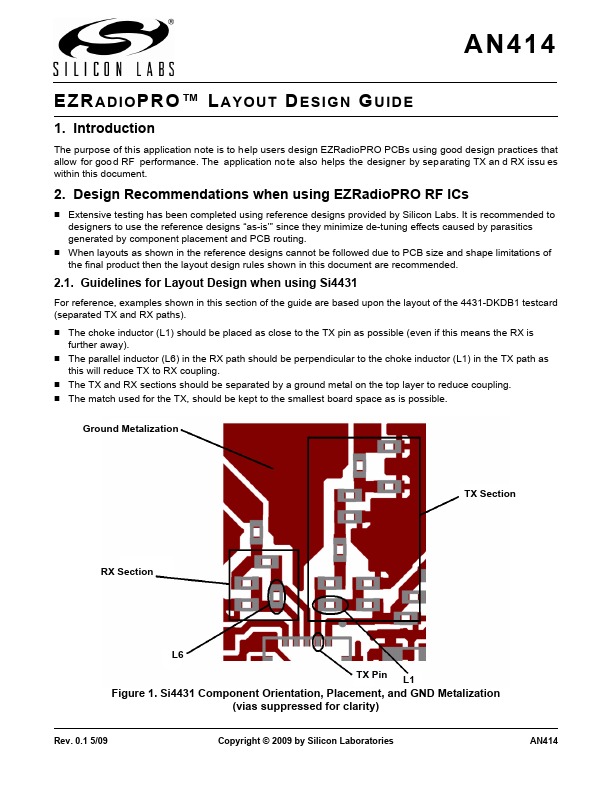
2.1. Guidelines for Layout Design when using Si4431
For reference, examples shown in this section of the guide are based upon the layout of the 4431-DKDB1 testcard (separated TX and RX paths). The choke inductor (L1) should be placed as close to the TX pin as possible (even if this means the RX is further away). The parallel inductor (L6) in the RX path should be perpendicular to the choke inductor (L1) in the TX path as this will reduce TX to RX coupling. The TX and RX sections should be separated by a ground metal on the top layer to reduce coupling. The match used for the TX, should be kept to the smallest board space as is possible.
Ground Metalization
...
Similar Datasheet