Data Sheet
FEATURES
Input voltage range: 2.4 V to 5.5 V Low standby current: 1 µA Switching frequency: 3 MHz I2C interfa...
Data Sheet
FEATURES
Input
voltage range: 2.4 V to 5.5 V Low standby current: 1 µA Switching frequency: 3 MHz I2C interface Synchronous Buck 1 regulator: 600 mA Synchronous Buck 2 regulator: 250 mA Low dropout regulator (LDO): 150 mA Internal compensation Internal soft start Thermal shutdown 20-lead 4 mm × 4 mm LFCSP
APPLICATIONS
Digital cameras, handsets Mobile TVs
GENERAL DESCRIPTION
The ADP5020 provides a highly integrated power solution that includes all of the power circuits necessary for a digital imaging module. It comprises two step-down dc-to-dc converters, one LDO, and a power sequence controller. All dc-to-dc converters integrate power p
MOSFETs and n
MOSFETs, making the system simpler and more compact and reducing the cost. The ADP5020 has digitally programmed output
voltages and buck converters that can source up to 600 mA. A fixed frequency operation of 3 MHz enables the use of tiny inductors and
capacitors. The buck converters use a
voltage mode, constant-frequency PWM control scheme, and the synchronous rectification is implemented to reduce the power loss. The Buck 1 regulator operates at up to 93% efficiency.
Power Management Unit for Imaging Modules ADP5020
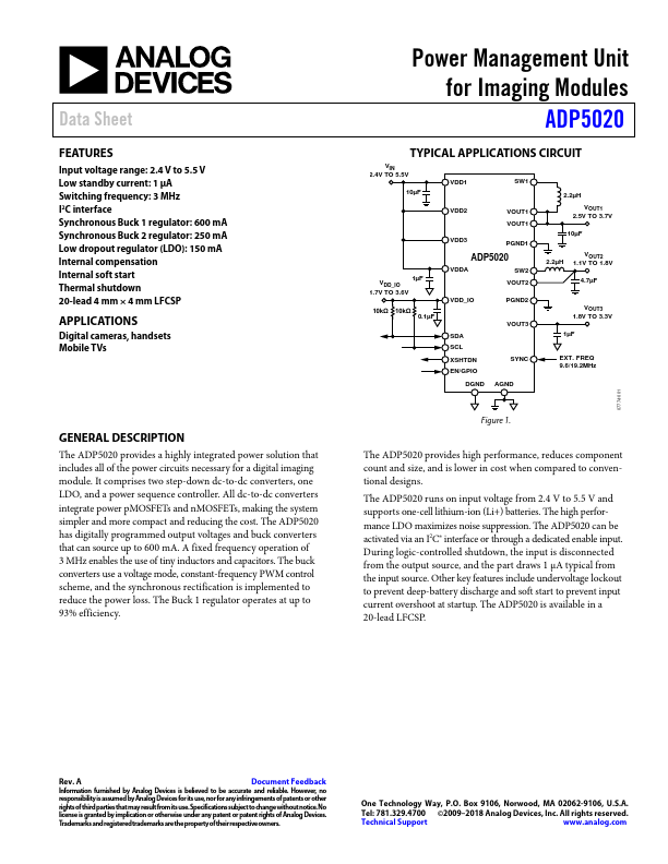
TYPICAL APPLICATIONS CIRCUIT
VIN 2.4V TO 5.5V
VDD1
SW1
10µF
2.2µH
1µF VDD_IO 1.7V TO 3.6V
10kΩ 10kΩ 0.1µF
VDD2
VOUT1 VOUT1
VDD3
PGND1
ADP5020
VDDA
SW2
VOUT2
VDD_IO
PGND2
SDA SCL XSHTDN EN/GPIO
VOUT3 SYNC
VOUT1 2.5V TO 3.7V 10µF
VOUT2 2.2µH 1.1V TO 1.8V
4.7µF
VOUT3 1.8V TO 3.3V 1µF
EXT. ...