DatasheetsPDF.com
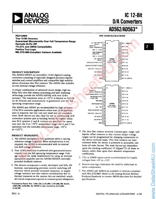
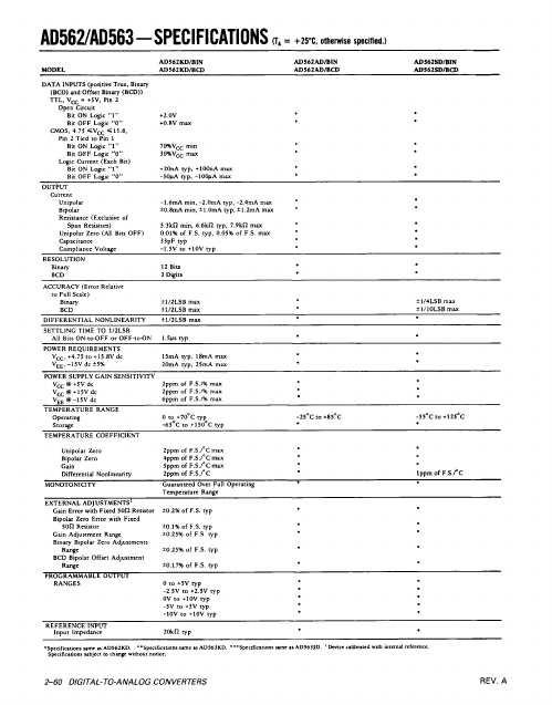
AD562
Part Number
AD562
Manufacturer
Analog Devices
Description
(AD562 / AD563) 12-Bit D/A Converter
Published
Dec 23, 2005
Datasheet
AD562
PDF File
Features
w www..com w w .D t a S a e h t e U 4 .c m o ...
Similar Datasheet
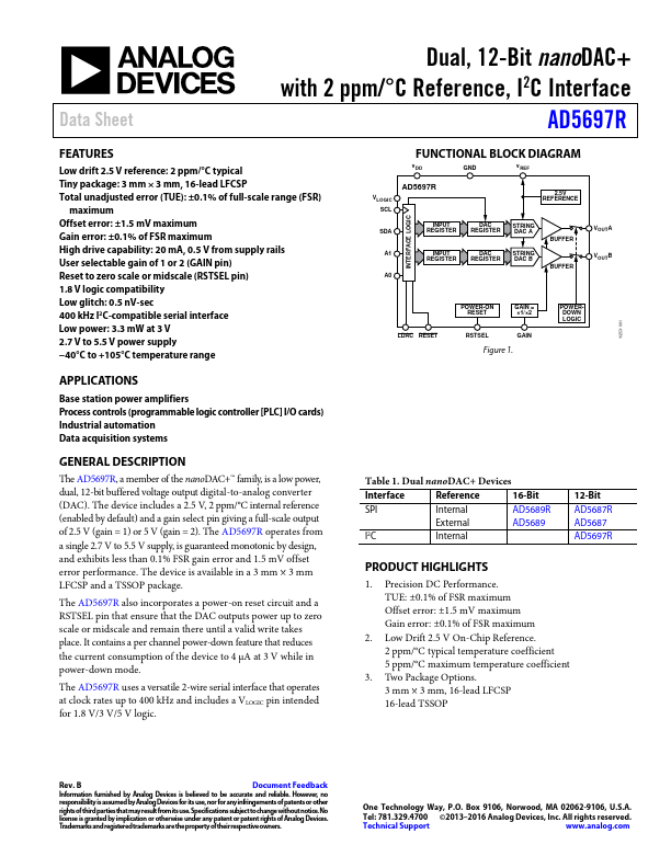
AD5697R
Dual 12-Bit nanoDAC+
(Analog Devices)
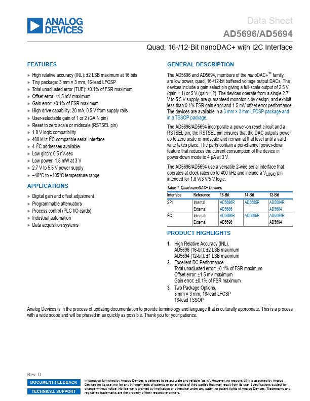
AD5696R
Quad 16-/14-/12-Bit nanoDAC+
(Analog Devices)
AD5696
16-/12-Bit nanoDAC+
(Analog Devices)
AD5695R
Quad 16-/14-/12-Bit nanoDAC+
(Analog Devices)
AD5694R
Quad 16-/14-/12-Bit nanoDAC+
(Analog Devices)
Since 2006. D4U Semicon,
Electronic Components Datasheet Search Site. (
Privacy Policy & Contact
)