a
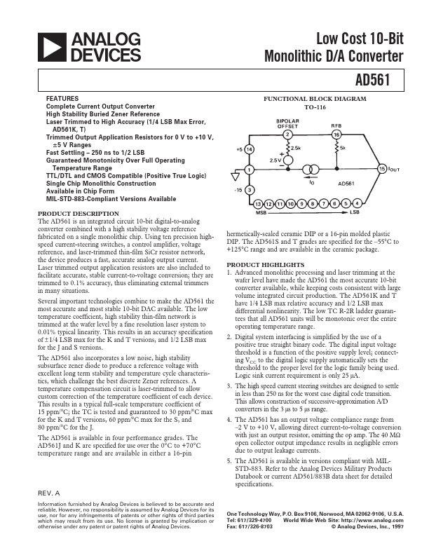
FEATURES Complete Current Output Converter High Stability Buried Zener Reference Laser Trimmed to High Accuracy (1/4 LSB Max Error, AD561K, T) Trimmed Output Application Resistors for 0 V to +10 V, ؎5 V Ranges Fast Settling – 250 ns to 1/2 LSB Guaranteed Monotonicity Over Full Operating Temperature Range TTL/DTL and CMOS Compatible (Positive True Logic) Si...