90SQ045 Datasheet
90SQ Series
Technical Data Data Sheet N1455, Rev.B
90SQ035/90SQ040/90SQ045 SCHOTTKY RECTIFIER
Features
DO-201AD
150°C TJ operation Low forward voltage drop High purity, high temperature epoxy encapsulation for
enhanced mechanical strength and moisture resistance High frequency operation Guard ring for enhanced ruggedness and long term
reliability Terminals finish: 100% Pure Tin This is a Pb − Free Device All SMC parts are traceable to the wafer lot Additional testing can be offered upon request
Circuit Diagram
Maximum Ratings:
Characteristics Peak Repetitive Reverse Voltage Working Peak Reverse Voltage DC Blocking Voltage Average Rectified Forward Current Peak One Cycle Non-Repetitive Surge Current Non-Repetitive Avalanche Energy Repetitive Avalanche Current
Applications
Switching power supply Converters Free-Wheeling diodes Reverse battery protection
Symbol VRRM VRWM VR
IF (AV)
IFSM EAS
IAR
Condition
-
50% duty cycle @TC = 69°C, rectangular wave form.
Part Number |
90SQ045 |
Manufacturers |
International Rectifier |
Logo |
|
Description |
SCHOTTKY RECTIFIER |
Datasheet |
90SQ045 Datasheet (PDF) |
Bulletin PD-2.222 rev. C 12/01
90SQ... SERIES
SCHOTTKY RECTIFIER 9 Amp
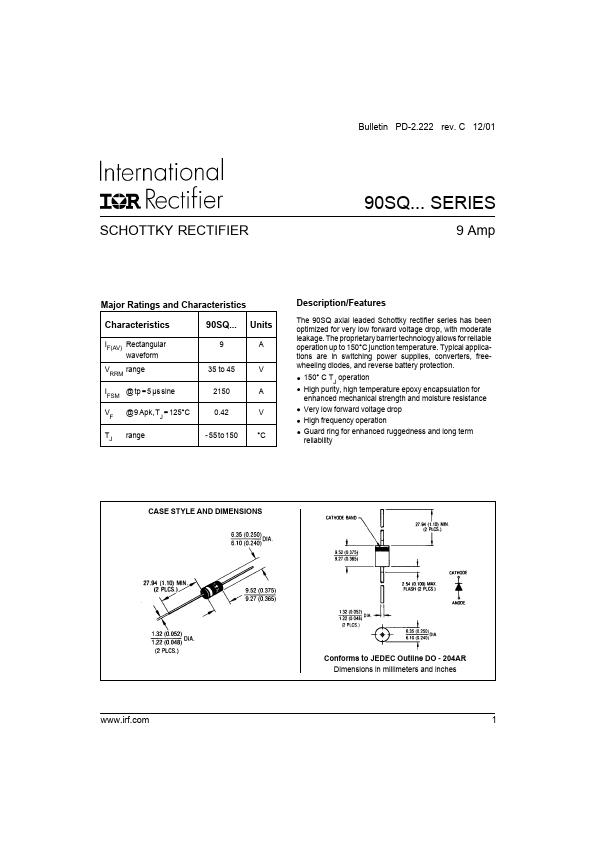
Major Ratings and Characteristics Characteristics
IF(AV) Rectangular waveform VRRM range IFSM @ tp = 5 µs sine VF TJ @ 9 Apk, TJ = 125°C range
Description/Features Units
A V A V °C The 90SQ axial leaded Schottky rectifier series has been optimized for very low forward voltage drop, with moderate leakage. The proprietary barrier technology allows for reliable operation up to 150°C junction temperature. Typical applications are in switching power supplies, converters, freewheeling diodes, and reverse battery protection. 150° C TJ operation High purity, high temperature epoxy encapsulation for enhanced mechanical strength.
SCHOTTKYRECTIFIER
90SQ Series
Technical Data Data Sheet N1455, Rev.B
90SQ035/90SQ040/90SQ045 SCHOTTKY RECTIFIER
Features
DO-201AD
150°C TJ operation Low forward voltage drop High purity, high temperature epoxy encapsulation for
enhanced mechanical strength and moisture resistance High frequency operation Guard ring for enhanced ruggedness and long term
reliability Terminals finish: 100% Pure Tin This is a Pb − Free Device All SMC parts are traceable to the wafer lot Additional testing can be offered upon request
Circuit Diagram
Maximum Ratings:
Characteristics Peak Repetitive Reverse Voltage Working Peak Reverse Voltage DC Blocking Voltage Average Rectified Forward Current Peak One Cycle Non-Repetitive Surge Current Non-Repetitive Avalanche Energy Repetitive Avalanche Current
Applications
Switching power supply Converters Free-Wheeling diodes Reverse battery protection
Symbol VRRM VRWM VR
IF (AV)
IFSM EAS
IAR
Condition
-
50% duty cycle @TC = 69°C, rectangular wave form 8.3 ms, half Sine pulse TJ=25℃,IAS=1.8A,L=7.4mH Current decaying linearly to zero in 1 μsec Frequency limited by TJ max. VA=1.5×VR typical
Max. 35(90SQ035) 40(90SQ040) 45(90SQ045)
9
340 12
1.8
Units V
A A mJ A
Electrical Characteristics:
Characteristics Forward Voltage Drop*
Reverse Current*
Junction Capacitance Voltage Rate of Change * Pulse width < 300 µs, duty cycle < 2%
Symbol VF1
VF2
IR1 IR2 CT dv/dt
Condition
@ 9A, Pulse, TJ = 25 C @ 18A, Pulse, TJ = 25 C @ 9A, Pulse, TJ = 125 C .
2024-02-15 : 150CMQ040 90SQ035 MUR1660 SM165KD800G2 90SQ040 90SQ045 150CMQ035 150CMQ045 MBR1060S SM165KE800G2