74V2T14
TRIPLE SCHMITT INVERTER
HIGH SPEED: tPD = 5.0ns (TYP.) at VCC = 5V LOW POWER DISSIPATION: ICC = 1µA(MAX.) at TA ...
74V2T14
TRIPLE SCHMITT INVERTER
HIGH SPEED: tPD = 5.0ns (TYP.) at VCC = 5V LOW POWER DISSIPATION: ICC = 1µA(MAX.) at TA = 25°C www.DataSheet4U.com s TYPICAL HYSTERESIS: Vh=700mV at VCC=4.5V s POWER DOWN PROTECTION ON INPUT s SYMMETRICAL OUTPUT IMPEDANCE: |IOH| = IOL = 8mA (MIN) at VCC = 4.5V s BALANCED PROPAGATION DELAYS: tPLH ≅ tPHL s OPERATING
VOLTAGE RANGE: VCC(OPR) = 4.5V to 5.5V s IMPROVED LATCH-UP IMMUNITY
s s
SOT23-8L
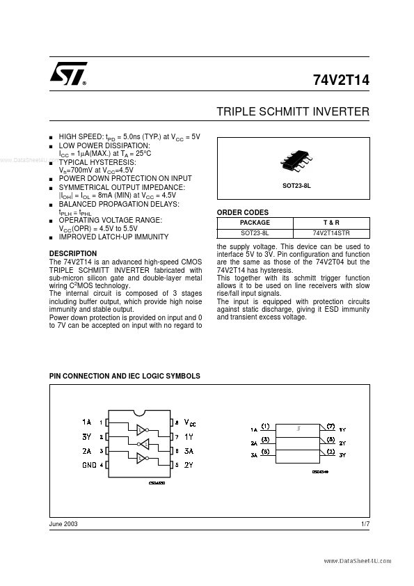
ORDER CODES
PACKAGE SOT23-8L T&R 74V2T14STR
DESCRIPTION The 74V2T14 is an advanced high-speed
CMOS TRIPLE SCHMITT INVERTER fabricated with sub-micron silicon gate and double-layer metal wiring C2MOS technology. The internal circuit is composed of 3 stages including buffer output, which provide high noise immunity and stable output. Power down protection is provided on input and 0 to 7V can be accepted on input with no regard to
the supply
voltage. This device can be used to interface 5V to 3V. Pin configuration and function are the same as those of the 74V2T04 but the 74V2T14 has hysteresis. This together with its schmitt trigger function allows it to be used on line receivers with slow rise/fall input signals. The input is equipped with protection circuits against static discharge, giving it ESD immunity and transient excess
voltage.
PIN CONNECTION AND IEC LOGIC SYMBOLS
June 2003
1/7
74V2T14
INPUT EQUIVALENT CIRCUIT PIN DESCRIPTION
PIN No 1, 3, 6 7, 5, 2 4 8 SYMBOL 1A, 2A, 3A 1Y, 2Y, 3Y GND VCC NAME QND FUNCTION Data Inputs Data Outputs Ground (0...