®
74V2G66
DUAL BILATERAL SWITCH
PRELIMINARY DATA
s
s
s
s
s
HIGH SPEED: tPD = 0.3 ns (TYP.) at VCC = 5V tPD = 0.4 ...
®
74V2G66
DUAL BILATERAL SWITCH
PRELIMINARY DATA
s
s
s
s
s
HIGH SPEED: tPD = 0.3 ns (TYP.) at VCC = 5V tPD = 0.4 ns (TYP.) at VCC = 3.3V LOW POWER DISSIPATION: ICC = 1 µA (MAX.) at TA = 25 oC LOW ”ON” RESISTANCE: RON = 10Ω (TYP.)AT VCC = 5.0V II/O=100µA RON = 12Ω (TYP.)AT VCC = 3.3V II/O=100µA SINE WAVE DISTORTION 0.04% (TYP.) AT VCC=3.3V f=1KHz WIDE OPERATING
VOLTAGE RANGE: VCC (OPR) = 2V to 5V
SOT23-8L
ORDER CODES PACKAGE SOT23-8L T UBE T& R 74V2G66STR
DESCRIPTION The 74V2G66 is an high-speed
CMOS DUAL BILATERAL SWITCH fabricated in silicon gate C2MOS technology. It achieves high speed propagation delay and VERY LOW ON resistances while maintaining true
CMOS low power consumption. This feature makes this part ideal for battery-powered equipment. This bilateral switch handles rail to rail analog and digital signals that may vary across the full
power-supply range (from Vcc to Ground). The C input is provided to control the switch and it’s compatible with standard
CMOS output; the switch is ON when the C input is held high and off when C is held low. It can be used in many application as Battery Powered System, Audio Signal Routing, Communications System, Test Equipment. It’s available in the commercial temperature range in SOT23-8L.
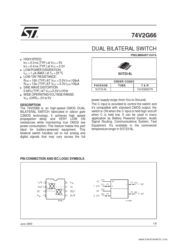
PIN CONNECTION AND IEC LOGIC SYMBOLS
June 2000
1/8
74V2G66
LOGIC DIAGRAM PIN DESCRIPTION
PIN No 1, 5 2, 6 3, 7 4 8 SYMBOL 1 to 2 I/O 1 to 2 O/I 1C to 2C GND VCC NAME AND FUNCT ION Independent Input/Output Independent Output/Input En...