DM74LS243 Quadruple Bus Transceiver
August 1986 Revised January 2000
DM74LS243 Quadruple Bus Transceiver
General Descr...
DM74LS243 Quadruple Bus Transceiver
August 1986 Revised January 2000
DM74LS243 Quadruple Bus Transceiver
General Description
This four data line transceiver is designed for asynchronous two-way communications between data buses. It can be used to drive terminated lines down to 133Ω.
Features
s Two-way asynchronous communication between data buses s PNP inputs reduce DC loading on bus line s Hysteresis at data inputs improves noise margin
Ordering Code:
Order Number DM74LS243M DM74LS243N Package Number M14A N14A Package Description 14-Lead Small Outline Integrated Circuit (SOIC), JEDEC MS-120, 0.150 Narrow 14-Lead Plastic Dual-In-Line Package (PDIP), JEDEC MS-001, 0.300 Wide
Devices also available in Tape and Reel. Specify by appending the suffix letter “X” to the ordering code.
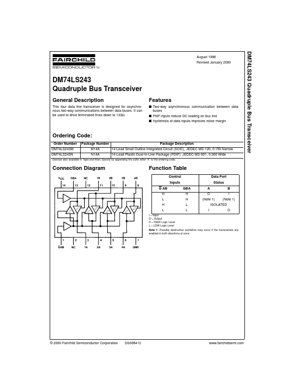
Connection Diagram
Function Table
Control Inputs G AB H L H L
I = Input O = Output H = HIGH Logic Level L = LOW Logic Level Note 1: Possibly destructive oscillation may occur if the transceivers are enabled in both directions at once.
Data Port Status GBA H H L L I A O (Note 1) ISOLATED O B I (Note 1)
© 2000 Fairchild Semiconductor Corporation
DS006412
www.fairchildsemi.com
DM74LS243
Absolute Maximum Ratings(Note 2)
Supply
Voltage Input
Voltage Any G A or B Operating Free Air Temperature Range Storage Temperature Range 7V 5.5V 0°C to +70°C −65°C to +150°C 7V
Note 2: The “Absolute Maximum Ratings” are those values beyond which the safety of the device cannot be guaranteed. The device should...