74ALVC16839 Low Voltage 20-Bit Selectable Register/Buffer with 3.6V Tolerant Inputs and Outputs
December 2001 Revised D...
74ALVC16839 Low
Voltage 20-Bit Selectable Register/Buffer with 3.6V Tolerant Inputs and Outputs
December 2001 Revised December 2001
74ALVC16839 Low
Voltage 20-Bit Selectable Register/Buffer with 3.6V Tolerant Inputs and Outputs
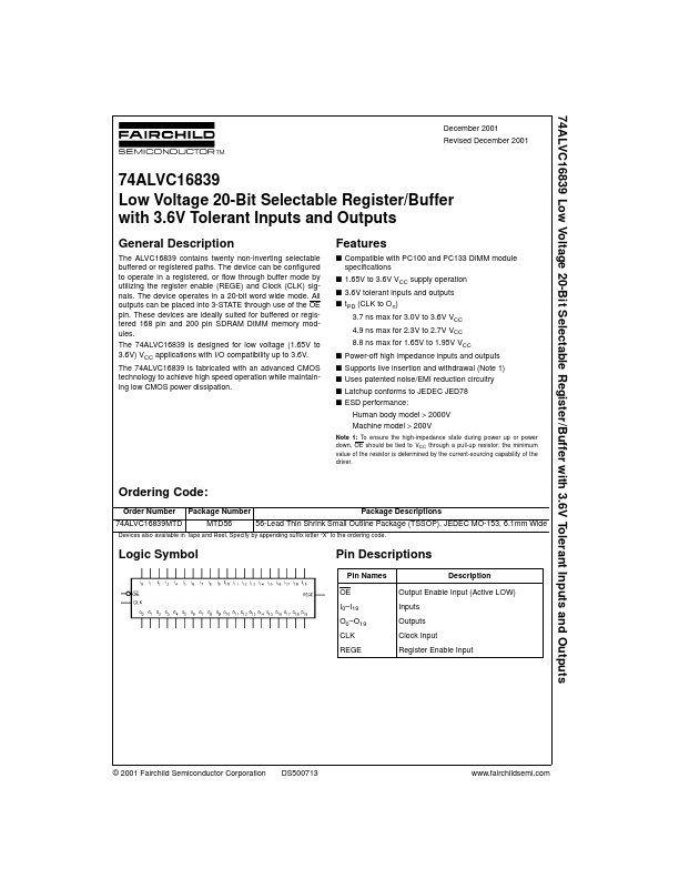
General Description
The ALVC16839 contains twenty non-inverting selectable buffered or registered paths. The device can be configured to operate in a registered, or flow through buffer mode by utilizing the register enable (REGE) and Clock (CLK) signals. The device operates in a 20-bit word wide mode. All outputs can be placed into 3-STATE through use of the OE pin. These devices are ideally suited for buffered or registered 168 pin and 200 pin SDRAM DIMM memory modules. The 74ALVC16839 is designed for low
voltage (1.65V to 3.6V) VCC applications with I/O compatibility up to 3.6V. The 74ALVC16839 is fabricated with an advanced
CMOS technology to achieve high speed operation while maintaining low
CMOS power dissipation.
Features
s Compatible with PC100 and PC133 DIMM module specifications s 1.65V to 3.6V VCC supply operation s 3.6V tolerant inputs and outputs s tPD (CLK to O n) 3.7 ns max for 3.0V to 3.6V VCC 4.9 ns max for 2.3V to 2.7V VCC 8.8 ns max for 1.65V to 1.95V VCC s Power-off high impedance inputs and outputs s Supports live insertion and withdrawal (Note 1) s Uses patented noise/EMI reduction circuitry s Latchup conforms to JEDEC JED78 s ESD performance: Human body model > 2000V Machine model > 200V
Note 1: To ensure the high-impedance sta...