74AC273 • 74ACT273 Octal D-Type Flip-Flop
November 1988 Revised August 2000
74AC273 • 74ACT273 Octal D-Type Flip-Flop
...
74AC273 74ACT273 Octal D-Type Flip-Flop
November 1988 Revised August 2000
74AC273 74ACT273 Octal D-Type Flip-Flop
General Description
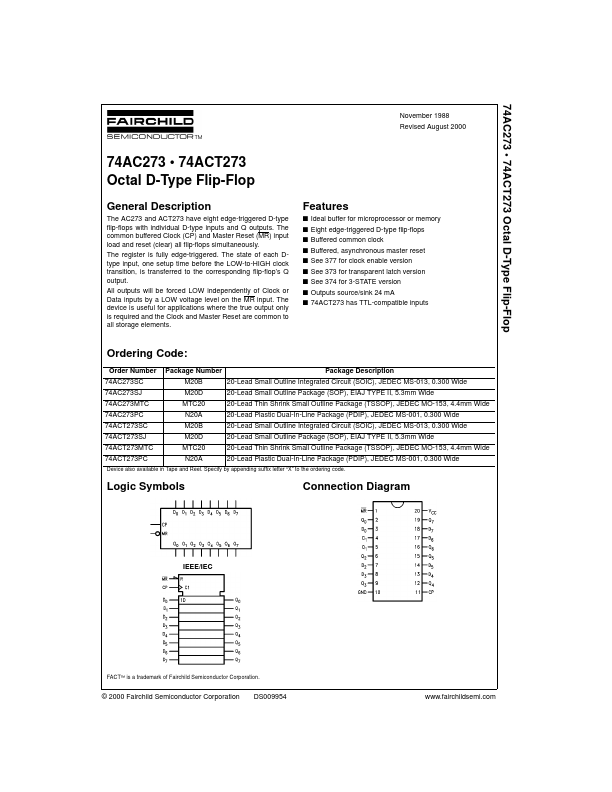
The AC273 and ACT273 have eight edge-triggered D-type flip-flops with individual D-type inputs and Q outputs. The common buffered Clock (CP) and Master Reset (MR) input load and reset (clear) all flip-flops simultaneously. The register is fully edge-triggered. The state of each Dtype input, one setup time before the LOW-to-HIGH clock transition, is transferred to the corresponding flip-flop’s Q output. All outputs will be forced LOW independently of Clock or Data inputs by a LOW
voltage level on the MR input. The device is useful for applications where the true output only is required and the Clock and Master Reset are common to all storage elements.
Features
s Ideal buffer for microprocessor or memory s Eight edge-triggered D-type flip-flops s Buffered common clock s Buffered, asynchronous master reset s See 377 for clock enable version s See 373 for transparent latch version s See 374 for 3-STATE version s Outputs source/sink 24 mA s 74ACT273 has TTL-compatible inputs
Ordering Code:
Order Number 74AC273SC 74AC273SJ 74AC273MTC 74AC273PC 74ACT273SC 74ACT273SJ 74ACT273MTC 74ACT273PC Package Number M20B M20D MTC20 N20A M20B M20D MTC20 N20A Package Description 20-Lead Small Outline Integrated Circuit (SOIC), JEDEC MS-013, 0.300 Wide 20-Lead Small Outline Package (SOP), EIAJ TYPE II, 5.3mm Wide 20-Lead Thin Shrink Small Outline Package (TSS...