• Inputs Are TTL-Voltage Compatible • 3-State Buffer-Type Outputs Drive Bus
Lines Directly
• Bus-Structured Pinout • Flo...
Inputs Are TTL-
Voltage Compatible 3-State Buffer-Type Outputs Drive Bus
Lines Directly
Bus-Structured Pinout Flow-Through Architecture to Optimize
PCB Layout
Center-Pin VCC and GND Configurations to
Minimize High-Speed Switching Noise
t EPIC (Enhanced-Performance Implanted
CMOS) 1-mm Process
500-mA Typical Latch-Up Immunity at
125°C
Package Options Include Plastic Small-
Outline Packages and Standard Plastic
300-mil DIPs
description
74ACT11873 DUAL 4-BIT D-TYPE LATCH
WITH 3–STATE OUTPUTS
SCAS096 – FEBRUARY 1990 – REVISED APRIL 1993
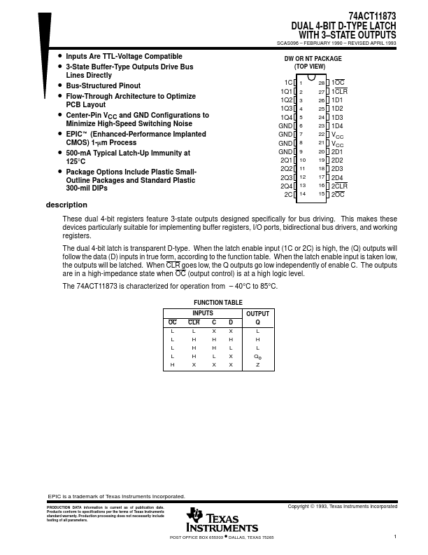
DW OR NT PACKAGE (TOP VIEW)
1C 1Q1 1Q2 1Q3 1Q4 GND GND GND GND 2Q1 2Q2 2Q3 2Q4
2C
1 2 3 4 5 6 7 8 9 10 11 12 13 14
28 1OC
27 1CLR
26 1D1
25 1D2
24 1D3
23 1D4 22 VCC 21 VCC 20 2D1 19 2D2 18 2D3 17 2D4 16 2CLR 15 2OC
These dual 4-bit registers feature 3-state outputs designed specifically for bus driving. This makes these devices particularly suitable for implementing buffer registers, I/O ports, bidirectional bus drivers, and working registers.
The dual 4-bit latch is transparent D-type. When the latch enable input (1C or 2C) is high, the (Q) outputs will follow the data (D) inputs in true form, according to the function table. When the latch enable input is taken low, the outputs will be latched. When CLR goes low, the Q outputs go low independently of enable C. The outputs are in a high-impedance state when OC (output control) is at a high logic level.
The 74ACT11873 is characterized for operation from – 40°C to 85°C.
FUNCTIO...