ą 74ACT11648 OCTAL BUS TRANSCEIVER AND REGISTER WITH 3ĆSTATE OUTPUTS
SCAS115 − D3458, MARCH 1990 − REVISED APRIL 1993
•...
ą 74ACT11648 OCTAL BUS TRANSCEIVER AND REGISTER WITH 3ĆSTATE OUTPUTS
SCAS115 − D3458, MARCH 1990 − REVISED APRIL 1993
Inputs Are TTL-
Voltage Compatible
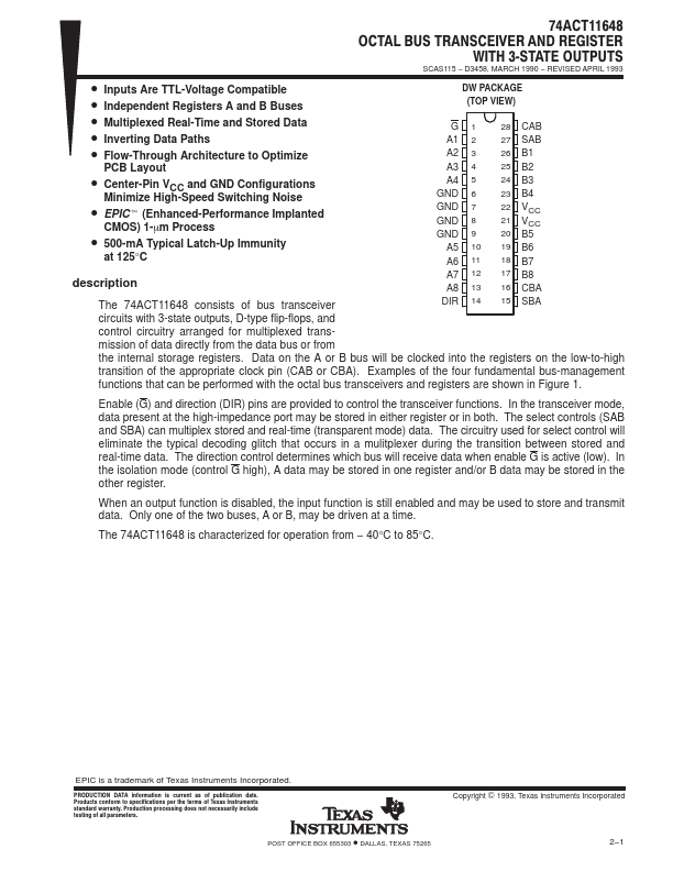
DW PACKAGE
Independent Registers A and B Buses
(TOP VIEW)
Multiplexed Real-Time and Stored Data Inverting Data Paths
G1 A1 2
28 CAB 27 SAB
Flow-Through Architecture to Optimize
A2 3
26 B1
PCB Layout
A3 4
25 B2
Center-Pin VCC and GND Configurations
Minimize High-Speed Switching Noise
EPICt (Enhanced-Performance Implanted
CMOS) 1-mm Process
500-mA Typical Latch-Up Immunity
at 125°C
A4 GND GND GND GND
A5 A6
5 6 7 8 9 10 11
24 B3
23 B4
22 VCC 21 VCC 20 B5 19 B6 18 B7
description
A7 12 A8 13
17 B8 16 CBA
The 74ACT11648 consists of bus transceiver
DIR 14 15 SBA
circuits with 3-state outputs, D-type flip-flops, and
control circuitry arranged for multiplexed trans-
mission of data directly from the data bus or from
the internal storage registers. Data on the A or B bus will be clocked into the registers on the low-to-high
transition of the appropriate clock pin (CAB or CBA). Examples of the four fundamental bus-management
functions that can be performed with the octal bus transceivers and registers are shown in Figure 1.
Enable (G) and direction (DIR) pins are provided to control the transceiver functions. In the transceiver mode, data present at the high-impedance port may be stored in either register or in both. The select controls (SAB and SBA) can multiplex stored and real-time (transpa...