74AC11652
OCTAL BUS TRANSCEIVER AND REGISTERS
WITH 3-STATE OUTPUTS
SCAS088A - DECEMBER 1989 - REVISED APRIL 1996
D Inde...
74AC11652
OCTAL BUS TRANSCEIVER AND REGISTERS
WITH 3-STATE OUTPUTS
SCAS088A - DECEMBER 1989 - REVISED APRIL 1996
D Independent Registers and Enables for A
and B Buses
DW PACKAGE (TOP VIEW)
D Multiplexed Real-Time and Stored Data D Inverting Data Paths D Flow-Through Architecture Optimizes PCB
Layout
D Center-Pin VCC and GND Configurations
Minimize High-Speed Switching Noise
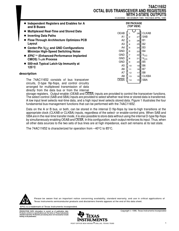
OEAB A1 A2 A3 A4
GND
1 2 3 4 5 6
28 CLKAB 27 SAB 26 B1 25 B2 24 B3 23 B4
D EPIC ™ (Enhanced-Performance Implanted
CMOS) 1-µm Process
D 500-mA Typical Latch-Up Immunity at
125°C
GND GND GND
A5 A6
7 8 9 10 11
22 VCC 21 VCC 20 B5
19 B6
18 B7
description
A7 12 A8 13
17 B8 16 CLKBA
The 74AC11652 consists of bus transceiver
OEBA 14 15 SBA
circuits, D-type flip-flops, and control circuitry
arranged for multiplexed transmission of data
directly from the data bus or from the internal
storage registers. Output-enable (OEAB and OEBA) inputs are provided to control the transceiver functions.
The select-control (SAB and SBA) inputs are provided to select whether real-time or stored data is transferred.
A low input level selects real-time data, and a high input level selects stored data. Figure 1 illustrates the four
fundamental bus-management functions that can be performed with the 74AC11652.
Data on the A or B bus, or both, can be stored in the internal D flip-flops by low-to-high transitions at the appropriate clock (CLKAB or CLKBA) inputs, regardless of the select- or enable-control pins. Whe...