• Contains Four Flip-Flops with Double-Rail
Outputs
• Clock Enable Latched to Avoid False
Clocking
• Applications Includ...
Contains Four Flip-Flops with Double-Rail
Outputs
Clock Enable Latched to Avoid False
Clocking
Applications Include: Buffer/Storage
Registers, Shift Registers, Pattern
Generators
Flow-Through Architecture Optimizes PCB
Layout
Center-Pin VCC and GND Pin
Configurations Minimize High-Speed
Switching Noise
EPIC (Enhanced-Performance Implanted
CMOS) 1-µm Process
500-mA Typical Latch-Up Immunity at
125°C
Package Options Include Plastic
Small-Outline Packages and Standard
Plastic 300-mil DIPs
74AC11379 QUAD D-TYPE FLIP-FLOP
WITH CLOCK ENABLE
SCAS104 − MARCH 1990 − REVISED APRIL 1993
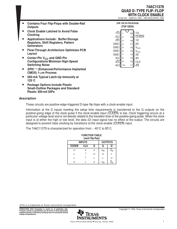
DW OR N PACKAGE (TOP VIEW)
1Q 2Q 2Q GND GND GND GND 3Q 3Q 4Q
1 2 3 4 5 6 7 8 9 10
20 1Q 19 CLKEN 18 1D 17 2D
16 VCC 15 VCC 14 3D 13 4D 12 CLK 11 4Q
description
These circuits are positive-edge-triggered D-type flip-flops with a clock-enable input.
Information at the D inputs meeting the setup time requirements is transferred to the Q outputs on the positive-going edge of the clock pulse if the clock-enable input (CLKEN) is low. Clock triggering occurs at a particular
voltage level and is not directly related to the transition time of the positive-going pulse. When the clock input is at either the high or low level, the data (D) input signal has no effect at the output. The circuits are designed to prevent false clocking by transitions at the clock-enable (CLKEN) input.
The 74AC11379 is characterized for operation from − 40°C to 85°C.
FUNCTION TABLE (each flip-flop)
INPUTS
OUTPUT...