M54HC273 M74HC273
OCTAL D TYPE FLIP FLOP WITH CLEAR
. . . . . . . .
HIGH SPEED fMAX = 67 MHz (TYP.) AT VCC = 5 V LOW P...
M54HC273 M74HC273
OCTAL D TYPE FLIP FLOP WITH CLEAR
. . . . . . . .
HIGH SPEED fMAX = 67 MHz (TYP.) AT VCC = 5 V LOW POWER DISSIPATION ICC = 4 µA (MAX.) AT TA = 25 °C HIGH NOISE IMMUNITY VNIH = VNIL = 28 % VCC (MIN.) OUTPUT DRIVE CAPABILITY 10 LSTTL LOADS SYMMETRICAL OUTPUT IMPEDANCE IOH = IOL = 4 mA (MIN.) BALANCED PROPAGATION DELAYS tPLH = tPHL WIDE OPERATING
VOLTAGE RANGE VCC (OPR) = 2 V TO 6 V PIN AND FUNCTION COMPATIBLE WITH 54/74LS273
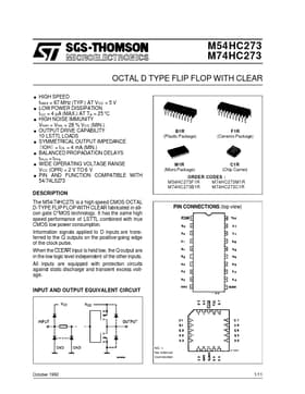
B1R (Plastic Package)
F1R (Ceramic Package)
M1R (Micro Package)
C1R (Chip Carrier)
ORDER CODES : M54HC273F1R M74HC273M1R M74HC273B1R M74HC273C1R
DESCRIPTION The M54/74HC273 is a high speed
CMOS OCTAL D-TYPE FLIP FLOP WITH CLEAR fabricated in silicon gate C2MOS technology. It has the same high speed performance of LSTTL combined with true
CMOS low power consumption. Information signals applied to D inputs are transferred to the Q outputs on the positive-going edge of the clock pulse. When the CLEAR input is held low, the Q output are in the low logic level independent of the other inputs. All inputs are equipped with protection circuits against static discharge and transient excess
voltage. INPUT AND OUTPUT EQUIVALENT CIRCUIT PIN CONNECTIONS (top view)
NC = No Internal Connection
October 1992
1/11
M54/M74HC273
PIN DESCRIPTION
PIN No 1 2, 5, 6, 9, 12, 15, 16, 19 3, 4, 7, 8, 13, 14, 17, 18 11 10 20 SYMBOL CLEAR Q0 to Q7 NAME AND FUNCTION Master Reset Input (Active LOW) Flip Flop Outputs
IEC LOGIC SYMBOL
D0 to D7
Data Inputs
...