2SK740
Silicon N-Channel MOS FET
Application
High speed power switching
Features
• • • • • Low on-resistance High spee...
2SK740
Silicon N-Channel MOS FET
Application
High speed power switching
Features
Low on-resistance High speed switching Low drive current No secondary breakdown Suitable for switching regulator, DC-DC converter and motor driver
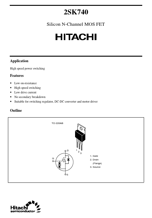
Outline
TO-220AB
D G
1
2
3 1. Gate 2. Drain (Flange) 3. Source
S
2SK740
Absolute Maximum Ratings (Ta = 25°C)
Item Drain to source
voltage Gate to source
voltage Drain current Drain peak current Body to drain diode reverse drain current Channel dissipation Channel temperature Storage temperature Notes: 1. PW ≤ 10 µs, duty cycle ≤ 1% 2. Value at TC = 25°C Symbol VDSS VGSS ID I D(pulse)* I DR Pch* Tch Tstg
2 1
Ratings 150 ±20 10 40 10 50 150 –55 to +150
Unit V V A A A W °C °C
Electrical Characteristics (Ta = 25°C)
Item Drain to source breakdown
voltage Gate to source breakdown
voltage Gate to source leak current Symbol Min V(BR)DSS V(BR)GSS I GSS 150 ±20 — — 2.0 — 4.0 — — — — — — — — — Typ — — — — — 0.12 7.0 1200 550 85 20 50 70 40 1.2 220 Max — — ±10 250 4.0 0.15 — — — — — — — — — — Unit V V µA µA V Ω S pF pF pF ns ns ns ns V ns I F = 10 A, VGS = 0 I F = 10 A, VGS = 0, diF/dt = 50 A/µs I D = 5 A, VGS = 10 V, RL = 6 Ω Test conditions I D = 10 mA, VGS = 0 I G = ±100 µA, VDS = 0 VGS = ±16 V, VDS = 0 VDS = 120 V, VGS = 0 I D = 1 mA, VDS = 10 V I D = 5 A, VGS = 10 V *1 I D = 5 A, VDS = 10 V *1 VDS = 10 V, VGS = 0, f = 1 MHz
Zero gate
voltage drain current I DSS Gate to source cutoff
voltage Static drain to source on state resistance Fo...