www.DataSheet4U.com
2SK3763
TOSHIBA Field Effect Transistor Silicon N Channel MOS Type ( -MOSIV)
2SK3763
unit•F‚•‚•
S...
www.DataSheet4U.com
2SK3763
TOSHIBA Field Effect Transistor Silicon N Channel MOS Type ( -MOSIV)
2SK3763
unitF‚‚
Switching Regulator Applications
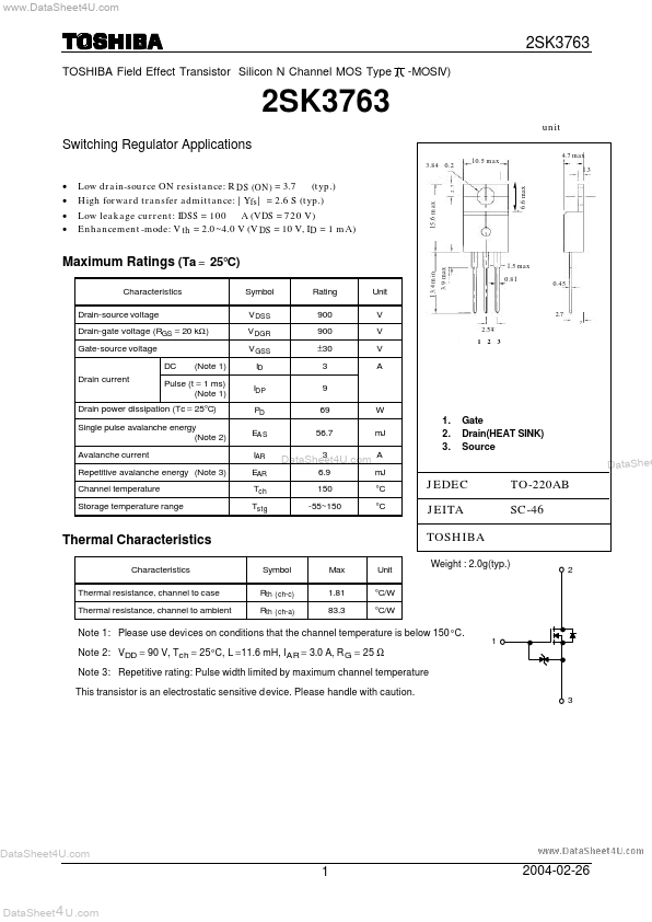
3.84} 0 .2
3.84}0.2
10.5 10.5max max
4.7max 4.7 max
1.3 6.6 max
6.6 max.
1.3
Low drain-source ON resistance: R DS (ON) = 3.7ƒ¶ (typ.) High forward transfer admittance: |Yfs| = 2.6 S (typ.) Low leakage current: IDSS = 100 ƒÊ A (V DS = 720 V) Enhancement-mode: V th = 2.0~4.0 V (V DS = 10 V, ID = 1 mA)
13.4 13.4 min min.
3.9 max
3.9 max.
Maximum Ratings (Ta = 25°C)
Characteristics Drain-source
voltage Drain-gate
voltage (RGS = 20 kΩ ) Gate-source
voltage DC Drain current (Note 1) Symbol V DSS V DGR V GSS ID IDP PD EA S IAR EAR Tch Tstg Pulse (t = 1 ms) (Note 1) Rating 900 900 ±30 3 9 69 56.7 W mJ A mJ °C °C Unit V V
15.6 max 15.6 max.
2.7
1.5 max 1.5 max 0.81
0.81 max
0.45
0.45
2.7
2.54 2.54 2.7
1
2
3
V A
Drain power dissipation (Tc = 25°C) Single pulse avalanche energy (Note 2) Avalanche current Repetitive avalanche energy (Note 3) Channel temperature Storage temperature range
DataSheet4U.com
6.9 150 -55~150
3
1. 2. 3.
Gate Drain(HEAT SINK) Source
DataShee
JEDEC JEITA TOSHIBA
TO-220AB SC-46
\
2
Thermal Characteristics
Characteristics Thermal resistance, channel to case Thermal resistance, channel to ambient Symbol Rth (ch-c) Rth (ch-a) Max 1.81 83.3 Unit °C/W °C/W
Weight : 2.0g(typ.)
Note 1: Please use devices on conditions that the channel temperature is below 150°C. Note 2: VDD = 90 V...