2SD467
Silicon NPN Epitaxial
Application
• Low frequency power amplifier • Complementary pair with 2SB561
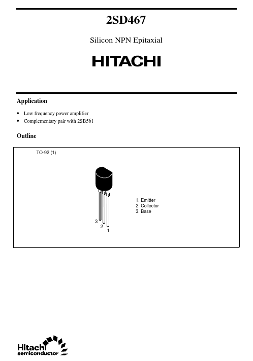
Outline
TO-9...
2SD467
Silicon NPN Epitaxial
Application
Low frequency power amplifier Complementary pair with 2SB561
Outline
TO-92 (1)
1. Emitter 2. Collector 3. Base 3 2 1
2SD467
Absolute Maximum Ratings (Ta = 25°C)
Item Collector to base
voltage Collector to emitter
voltage Emitter to base
voltage Collector current Collector peak current Collector power dissipation Junction temperature Storage temperature Symbol VCBO VCEO VEBO IC iC(peak) PC Tj Tstg Ratings 25 20 5 0.7 1.0 0.5 150 –55 to +150 Unit V V V A A W °C °C
Electrical Characteristics (Ta = 25°C)
Item Collector to base breakdown
voltage Symbol V(BR)CBO Min 25 20 5 —
1
Typ — — — — — 0.19 0.76 280 12
Max — — — 1.0 240 0.5 1.0 — —
Unit V V V µA
Test conditions I C = 10 µA, IE = 0 I C = 1 mA, RBE = ∞ I E = 10 µA, IC = 0 VCB = 20 V, IE = 0 VCE = 1 V, IC = 0.15 A (Pulse test)
Collector to emitter breakdown V(BR)CEO
voltage Emitter to base breakdown
voltage Collector cutoff current DC current transfer ratio Collector to emitter saturation
voltage Base to emitter
voltage Gain bandwidth product Collector output capacitance Note: B 85 to170 C 120 to 240 V(BR)EBO I CBO hFE*
85 — — — —
VCE(sat) VBE fT Cob
V V MHz pF
I C = 0.5 A, IB = 0.05 A (Pulse test) VCE = 1 V, IC = 0.15 A (Pulse test) VCE = 1 V, IC = 0.15 A (Pulse test) VCB = 10 V, IE = 0, f = 1 MHz
1. The 2SD467 is grouped by h FE as follows.
2
2SD467
Typical Output Characteristics Maximum Collector Dissipation Curve 0.6 Collector Power Dissipation PC (W) Collector Cu...