2SD2121(L)/(S)
Silicon NPN Epitaxial
Application
Low frequency power amplifier complementary pair with 2SB1407(L)/(S)
...
2SD2121(L)/(S)
Silicon NPN Epitaxial
Application
Low frequency power amplifier complementary pair with 2SB1407(L)/(S)
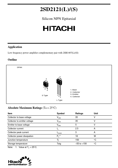
Outline
DPAK
4 4
1
2
3 12
S Type
3
1. Base 2. Collector 3. Emitter 4. Collector
L Type
Absolute Maximum Ratings (Ta = 25°C)
Item Collector to base
voltage Collector to emitter
voltage Emitter to base
voltage Collector current Collector peak current Collector power dissipation Junction temperature Storage temperature Note: 1. Value at TC = 25°C. Symbol VCBO VCEO VEBO IC I C(peak) PC * Tj Tstg
1
Ratings 35 35 5 2.5 3 18 150 –55 to +150
Unit V V V A A W °C °C
2SD2121(L)/(S)
Electrical Characteristics (Ta = 25°C)
Item Collector to base breakdown
voltage Symbol V(BR)CBO Min 35 35 5 —
1
Typ — — — — — — — —
Max — — — 20 320 — 1.5 1.0
Unit V V V µA
Test conditions I C = 1 mA, IE = 0 I C = 10 mA, RBE = ∞ I E = 1 mA, IC = 0 VCB = 35 V, IE = 0 VCE = 2 V, IC = 0.5 A*2 VCE = 2 V, IC = 1.5 A*2 VCE = 2 V, IC = 1.5 A*2 I C = 2 A, IB = 0.2 A*2
Collector to emitter breakdown V(BR)CEO
voltage Emitter to base breakdown
voltage Collector cutoff current DC current transfer ratio V(BR)EBO I CBO hFE1* hFE2 Base to emitter
voltage Collector to emitter saturation
voltage VBE VCE(sat)
60 20 — —
V V
Notes: 1. The 2SD2121(L)/(S) is grouped by hFE1 as follows. B 60 to 120 C 100 to 200 D 160 to 320
2. Pulse test.
Maximum Collector Dissipation Curve 30 Collector power dissipation PC (W) 10
Area of Safe Operation
Collector current IC (A)
20
3.0
iC(peak) IC(max)
P...