2SC3365
Silicon NPN Triple Diffused
Application
High voltage, high speed and high power switching
Outline
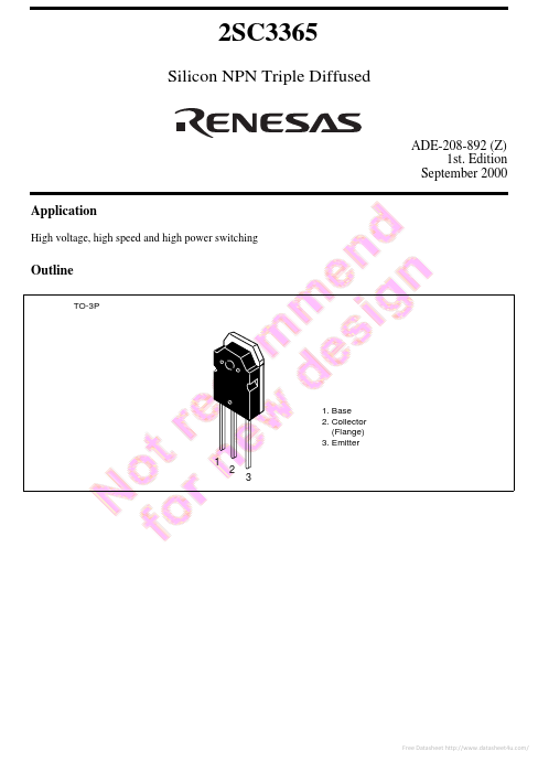
TO-3P
ADE-20...
2SC3365
Silicon NPN Triple Diffused
Application
High
voltage, high speed and high power switching
Outline
TO-3P
ADE-208-892 (Z) 1st. Edition
September 2000
1 2 3
1. Base 2. Collector
(Flange) 3. Emitter
Free Datasheet http://www.datasheet4u.com/
2SC3365
Absolute Maximum Ratings (Ta = 25°C)
Item Collector to base
voltage Collector to emitter
voltage Emitter to base
voltage Collector current Collector peak current Base current Collector power dissipation Junction temperature Storage temperature Note: 1. Value at TC = 25°C
Symbol VCBO VCEO VEBO IC I C(peak) IB PC * 1 Tj Tstg
Ratings
Unit
500
V
400
V
10
V
10
A
20
A
5
A
80
W
150
°C
–55 to +150
°C
Electrical Characteristics (Ta = 25°C)
Item Collector to emitter sustain
voltage
Symbol Min
VCEO(sus) VCEX(sus)
400 400
Typ — —
Emitter to base breakdown
V(BR)EBO
10
—
voltage
Collector cutoff current
I CBO
—
—
I CEO
—
—
DC current transfer ratio
hFE1
12
—
hFE2
5
—
Collector to emitter saturation VCE(sat)
—
—
voltage
Base to emitter saturation
VBE(sat)
—
—
voltage
Turn on time Storage time Fall time Note: 1. Pulse test
t on
—
—
t stg
—
—
tf
—
—
Max Unit
—
V
—
V
—
V
50
µA
50
µA
—
—
1.0 V
1.5 V
1.0 µs 2.5 µs 1.0 µs
Test conditions IC = 0.2 A, RBE = ∞, L = 100 mH IC = 10 A, IB1 = 2 A, IB2 = –0.6 A, VBE = –5.0 V, L = 180 µH, Clamped IE = 10 mA, IC = 0
VCB = 400 V, IE = 0 VCE = 350 V, RBE = ∞ VCE = 5.0 V, IC = 5 A*1 VCE = 5.0 V, IC = 10 A*1 IC = 5 A, IB =...