2SC1881(K)
Silicon NPN Triple Diffused
Application
High gain amplifier power switching
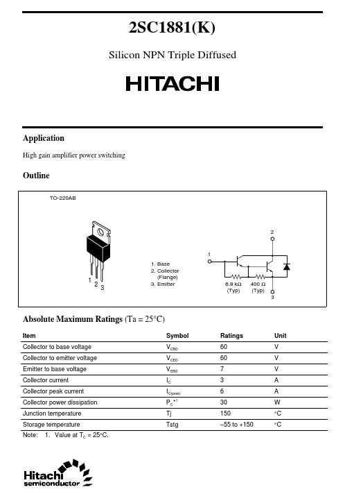
Outline
TO-220AB
2
1 1. Base ...
2SC1881(K)
Silicon NPN Triple Diffused
Application
High gain amplifier power switching
Outline
TO-220AB
2
1 1. Base 2. Collector (Flange) 3. Emitter
1
2 3
6.8 kΩ (Typ)
400 Ω (Typ) 3
Absolute Maximum Ratings (Ta = 25°C)
Item Collector to base
voltage Collector to emitter
voltage Emitter to base
voltage Collector current Collector peak current Collector power dissipation Junction temperature Storage temperature Note: 1. Value at TC = 25°C. Symbol VCBO VCEO VEBO IC I C(peak) PC * Tj Tstg
1
Ratings 60 60 7 3 6 30 150 –55 to +150
Unit V V V A A W °C °C
2SC1881(K)
Electrical Characteristics (Ta = 25°C)
Item Symbol Min 60 7 — — 1000 500 Collector to emitter saturation
voltage Turn on time Turn off time Note: 1. Pulse test. VCE(sat) t on t off — — — Typ — — — — — — — 1 5 Max — — 0.2 0.4 — — 1.2 — — V µs µs Unit V V mA mA Test conditions I C = 50 mA, RBE = ∞ I E = 50 mA, IC = 0 VCB = 60 V, IE = 0 VCE = 30 V, RBE = ∞ VCE = 1.5 V I C = 1.5 A*1 I C = 2.5 A*1 I C = 2.5 A, IB = 20 mA*1 VCC = 11 V, IC = 2 A, I B1 = –IB2 = 8 mA Collector to emitter breakdown V(BR)CEO
voltage Emitter to base breakdown
voltage Collector cutoff current V(BR)EBO I CBO I CEO DC current transfer ratio hFE
Area of Safe Operation Maximum Collector Dissipation Curve 30 Collector power dissipation PC (W) Collector current IC (A) 10 iC (peak) 5 IC max 2
s 0m =1 pw on rati Ope C) DC = 25° (T C
20
1.0 0.5 0.2 0.1
10
Ta = 25°C 1 shot pulse
0
50 100 Case temperature TC (°C)
150
0.05 1
2
5
10
20
50...