2SB1391
Silicon PNP Triple Diffused
Application
Power switching
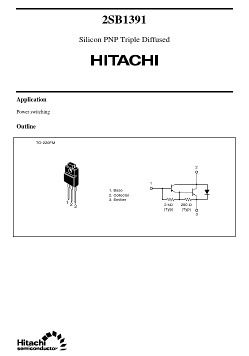
Outline
TO-220FM
2
1 1. Base 2. Collector 3. Emitter...
2SB1391
Silicon PNP Triple Diffused
Application
Power switching
Outline
TO-220FM
2
1 1. Base 2. Collector 3. Emitter
12 3
2 kΩ (Typ)
200 Ω (Typ) 3
2SB1391
Absolute Maximum Ratings (Ta = 25°C)
Item Collector to base
voltage Collector to emitter
voltage Emitter to base
voltage Collector current Collector peak current Collector power dissipation Symbol VCBO VCEO VEBO IC I C(peak) PC PC * Junction temperature Storage temperature Note: 1. Value at TC = 25°C. Tj Tstg
1
Ratings –120 –120 –7 –8 –12 2 25 150 –55 to +150
Unit V V V A A W °C °C
Electrical Characteristics (Ta = 25°C)
Item Collector to base breakdown
voltage Symbol V(BR)CBO Min –120 –120 –7 — — 1000 — — — — Typ — — — — — — — — — — Max — — — –10 –10 20000 –1.5 –3.0 –2.0 –3.5 V V Unit V V V µA Test conditions I C = –0.1 mA, IE = 0 I C = –25 mA, RBE = ∞ I E = –50 mA, IC = 0 VCB = –100 V, IE = 0 VCE = –100 V, RBE = ∞ VCE = –3 V, IC = –4 A*1 I C = –4 A, IB = –8 mA*1 I C = –8 A, IB = –80 mA*1 I C = –4 A, IB = –8 mA*1 I C = –8 A, IB = –80 mA*1
Collector to emitter breakdown V(BR)CEO
voltage Emitter to base breakdown
voltage Collector cutoff current V(BR)EBO I CBO I CEO DC current transfer ratio Collector to emitter saturation
voltage Base to emitter saturation
voltage Note: 1. Pulse test. hFE VCE(sat)1 VCE(sat)2 VBE(sat)1 VBE(sat)2
See switching characteristic curve of 2SB791(K).
2
2SB1391
Maximum Collector Dissipation Curve 30 Collector power dissipation Pc (W) Area of Safe Operation –20 i C (peak) –10 Collector ...