2SB1026
Silicon PNP Epitaxial
Application
• Low frequency power amplifier • Complementary pair with 2SD1419
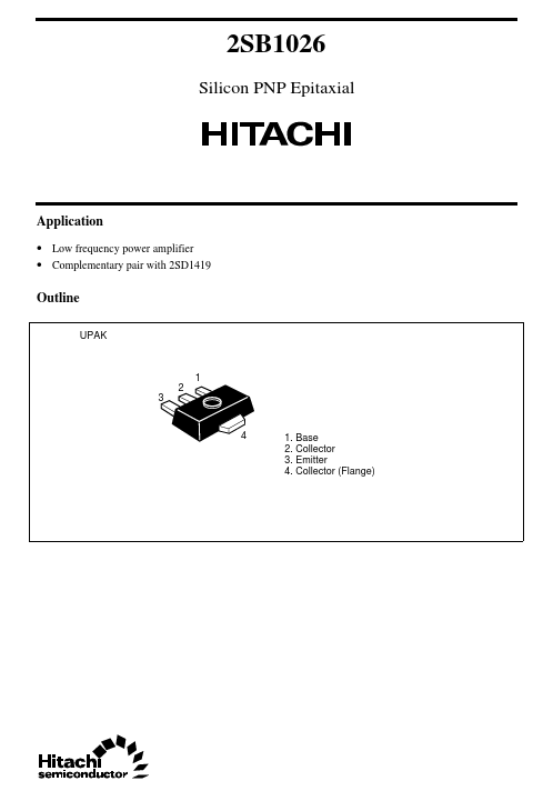
Outline
UP...
2SB1026
Silicon PNP Epitaxial
Application
Low frequency power amplifier Complementary pair with 2SD1419
Outline
UPAK
1 3 2
4
1. Base 2. Collector 3. Emitter 4. Collector (Flange)
2SB1026
Absolute Maximum Ratings (Ta = 25°C)
Item Collector to base
voltage Collector to emitter
voltage Emitter to base
voltage Collector current Collector peak current Collector power dissipation Junction temperature Storage temperature Symbol VCBO VCEO VEBO IC iC(peak)* PC * Tj Tstg
2 1
Ratings –120 –100 –5 –1 –2 1 150 –55 to +150
Unit V V V A A W °C °C
Notes: 1. PW ≤ 10 ms, Duty cycle ≤ 20% 2. Value on the alumina ceramic board (12.5 × 20 × 0.7 mm)
Electrical Characteristics (Ta = 25°C)
Item Collector to base breakdown
voltage Collector to emitter breakdown
voltage Emitter to base breakdown
voltage Collector cutoff current DC current transfer ratio Symbol V(BR)CBO V(BR)CEO V(BR)EBO I CBO hFE1* hFE2 Collector to emitter saturation
voltage Base to emitter
voltage Gain bandwidth product Collector output capacitance Note: Mark hFE1 VCE(sat) VBE fT Cob
1
Min –120 –100 –5 — 60 30 — — — —
Typ — — — — — — — — 140 20
Max — — — –10 200 — –1 –0.9 — —
Unit V V V µA
Test conditions I C = –10 µA, IE = 0 I C = –1 mA, RBE = ∞ I E = –10 µA, IC = 0 VCB = –100 V, IE = 0 VCE = –5 V, IC = –150 mA VCE = –5 V, I C = –500 mA (Pulse test)
V V MHz pF
I C = –500 mA, I B = –50 mA (Pulse test) VCE = –5 V, IC = –150 mA VCE = –5 V, IC = –150 mA VCB = –10 V, IE = 0, f = 1 MHz
1. The 2SB1026 is grouped by h...