2SA673A(K)
Silicon PNP Epitaxial
Application
• Low frequency amplifier • Medium speed switching
Outline
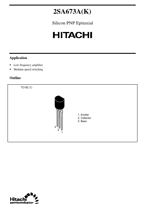
TO-92 (1)
1. ...
2SA673A(K)
Silicon PNP Epitaxial
Application
Low frequency amplifier Medium speed switching
Outline
TO-92 (1)
1. Emitter 2. Collector 3. Base 3 2 1
2SA673A(K)
Absolute Maximum Ratings (Ta = 25°C)
Item Collector to base
voltage Collector to emitter
voltage Emitter to base
voltage Collector current Collector power dissipation Junction temperature Storage temperature Symbol VCBO VCEO VEBO IC PC Tj Tstg Ratings –50 –50 –4 –0.5 0.4 150 –55 to +150 Unit V V V A W °C °C
2
2SA673A(K)
Electrical Characteristics (Ta = 25°C)
Item Collector to base breakdown
voltage Symbol V(BR)CBO Min –50 –50 –4 — — — — — 60 10 — — — — Typ — — — — — –0.64 –0.2 –0.87 — — 120 0.3 0.6 0.4 Max — — — –0.5 –0.5 — –0.6 — 320 — — — — — MHz µs µs µs Unit V V V µA µA V V V Test conditions I C = –10 µA, IE = 0 I C = –1 mA, RBE = ∞ I E = –10 µA, IC = 0 VCB = –20 V, IE = 0 VEB = –3 V, IC = 0 VEB = –3 V, IC = –10 mA I C = –150 mA, IB = –15 mA*2 I C = –150 mA, IB = –15 mA*2 VCE = –3 V, IC = –10 mA VCE = –3 V, IC = –500 mA*2 VCE = –3 V, IC = –10 mA VCC = –10.3 V I C = 10 IB1 = –10 IB2 = –10 mA VCC = –5 V, I C = IB1 = IB2 = –20 mA
Collector to emitter breakdown V(BR)CEO
voltage Emitter to base breakdown
voltage Collector cutoff current Emitter cutoff current Base to emitter
voltage Collector to emitter saturation
voltage Base to emitter saturation
voltage DC current transfer ratio V(BR)EBO I CBO I EBO VBE VCE(sat) VBE(sat) hFE*1 hFE Gain bandwidth product Turn on time Turn off time Storage time fT t on t off ...