2SA1468
Silicon PNP Epitaxial
Application
High voltage amplifier
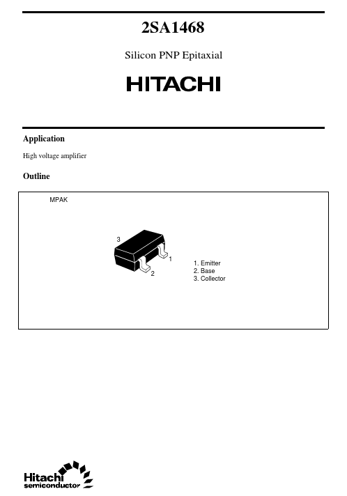
Outline
MPAK
3 1 2
1. Emitter 2. Base 3. Collector
...
2SA1468
Silicon PNP Epitaxial
Application
High
voltage amplifier
Outline
MPAK
3 1 2
1. Emitter 2. Base 3. Collector
2SA1468
Absolute Maximum Ratings (Ta = 25°C)
Item Collector to base
voltage Collector to emitter
voltage Emitter to base
voltage Collector current Collector power dissipation Junction temperature Storage temperature Symbol VCBO VCEO VEBO IC PC Tj Tstg Ratings –180 –180 –5 –100 150 150 –55 to +150 Unit V V V mA mW °C °C
Electrical Characteristics (Ta = 25°C)
Item Collector to base breakdown
voltage Symbol V(BR)CBO Min –180 –180 –5 100 — — — — Typ — — — — — — 200 3.5 Max — — — 320 –0.5 –1.0 — — V V MHz pF Unit V V V Test conditions I C = –10 µA, IE = 0 I C = –0.5 mA, RBE = ∞ I E = –10 µA, IC = 0 VCE = –12 V, IC = –2 mA*2 I C = –30 mA, IB = –3 mA*2 VCE = –12 V, IC = –2 mA VCE = –12 V, IC = –10 mA VCB = –10 V, IE = 0, f = 1 MHz
Collector to emitter breakdown V(BR)CEO
voltage Emitter to base breakdown
voltage DC current transfer ratio Collector to emitter saturation
voltage Base to emitter
voltage Gain bandwidth product Collector output capacitance V(BR)EBO hFE*1 VCE(sat) VBE fT Cob
Notes: 1. The 2SA1468 is grouped by h FE as follows. 2. Pulse test Grade Mark hFE B INB 100 to 200 C INC 160 to 320
2
2SA1468
Maximum Collector Dissipation Curve Collector Power Dissipation PC (mW) 150 –100 Collector Current IC (mA) Typical Output Characteristics
–1 0
–5
=1
.0
–2. 0
–80 –60
PC
100
–1.0
–0.5
50 mW
–40 –20 IB = 0
50
–0.2
–0.1 mA
Ta = 25°C
0
100 150 50...