2SA1390
Silicon PNP Epitaxial
Application
Low frequency amplifier
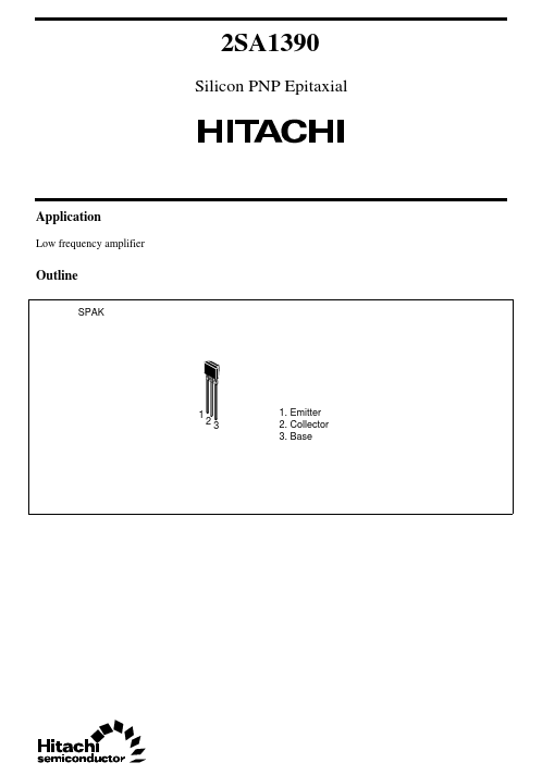
Outline
SPAK
1
23
1. Emitter 2. Collector 3. Base...
2SA1390
Silicon PNP Epitaxial
Application
Low frequency amplifier
Outline
SPAK
1
23
1. Emitter 2. Collector 3. Base
2SA1390
Absolute Maximum Ratings (Ta = 25°C)
Item Collector to base
voltage Collector to emitter
voltage Emitter to base
voltage Collector current Collector power dissipation Junction temperature Storage temperature Symbol VCBO VCEO VEBO IC PC Tj Tstg Ratings –35 –35 –4 –500 300 150 –55 to +150 Unit V V V mA mW °C °C
Electrical Characteristics (Ta = 25°C)
Item Collector to base breakdown
voltage Symbol V(BR)CBO Min –35 –35 –4 — — 60 10 — Typ — — — — –0.2 — — –0.64 Max — — — –0.5 –0.6 320 — — V Unit V V V µA V Test conditions I C = –10 µA, IE = 0 I C = –1 mA, RBE = ∞ I E = –10 µA, IC = 0 VCB = –20 V, IE = 0 I C = –150 mA, IB = –15 mA*2 VCE = –3 V, IC = –10 mA VCE = –3 V, IC = –500 mA*2 VCE = –3 V, IC = –10 mA
Collector to emitter breakdown V(BR)CEO
voltage Emitter to base breakdown
voltage Collector cutoff current Collector to emitter saturation
voltage DC current transfer ratio DC current transfer ratio Base to emitter
voltage V(BR)EBO I CBO VCE(sat) hFE1* 1 hFE2 VBE
Notes: 1. The 2SA1390 is grouped by hFE1 as follows. 2. Pulse test B 60 to 120 C 100 to 200 D 160 to 320
See characteristic curves of 2SA673.
2
2SA1390
Maximum Collector Dissipation Curve Collector Power Dissipation PC (mW) 300
200
100
0
100 150 50 Ambient Temperature Ta (°C)
3
4.2 Max 1.8 Max 3.2 Max
2.2 Max
Unit: mm
0.45 ± 0.1
14.5 Min
0.6
0.6 Max
0.4 ± 0.1
1.27 1.27
2.5...