2N7002DW
Dual N-Channel MOSFET
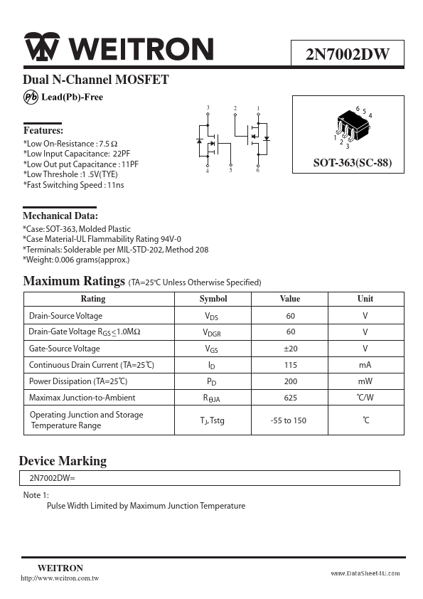
3 2 1
6 5
4
Features:
*Low On-Resistance : 7.5 Ω *Low Input Capacitance: 22PF *Low Out...
2N7002DW
Dual N-Channel
MOSFET
3 2 1
6 5
4
Features:
*Low On-Resistance : 7.5 Ω *Low Input Capacitance: 22PF *Low Out put Capacitance : 11PF *Low Threshole :1 .5V(TYE) *Fast Switching Speed : 11ns
1
2
3
4
5
6
SOT-363(SC-88)
Mechanical Data:
*Case: SOT-363, Molded Plastic *Case Material-UL Flammability Rating 94V-0 *Terminals: Solderable per MIL-STD-202, Method 208 *Weight: 0.006 grams(approx.)
Maximum Ratings (TA=25 C Unless Otherwise Specified)
Rating Drain-Source
Voltage Drain-Gate
Voltage R GS <1.0M Ω _ Gate-Source
Voltage Continuous Drain Current (TA=25 C) Power Dissipation (TA=25 C) Maximax Junction-to-Ambient Operating Junction and Storage Temperature Range Symbol VDS VDGR VGS ID PD R θJA TJ, Tstg Value 60 60 ±20 115 200 625 -55 to 150 Unit V V V mA mW C/W C
Device Marking
2N7002DW= Note 1: Pulse Width Limited by Maximum Junction Temperature
WEITRON
http://www.weitron.com.tw
2N7002DW
Electrical Characteristics
Characteristic (TA=25 C Unless otherwise noted) Symbol Min Typ Max Unit
Static
Drain-Source Breakdown
Voltage VGS=0V, ID=10 uA Gate-Threshold
Voltage VDS=V GS , ID =-250uA Gate-body Leakage +20V, VDS=0V VGS= _ Zero Gate
Voltage Drain Current VDS=60V, VGS=0V @ Tc=25 C VDS=60V, VGS=0V @ Tc=125 C On-State Drain Current VGS=10V, VDS=7.5V Drain-Source On-Resistance VGS=5V, ID=0.05A @ Tj=25 C VGS=10V, ID=0.5A @ Tj =125 C Forward Transconductance VDS=10V, ID=0.2A V(BR)DSS VGS (th) IGSS IDSS ID (on) 60 1.0 70 1.5 1.0 3.2 4.4 2.0 + _ 10 1.0 500 V V nA uA A ...