2N6052
Preferred Device
Darlington Complementary Silicon Power Transistors
This package is designed for general−purpos...
2N6052
Preferred Device
Darlington Complementary Silicon Power Transistors
This package is designed for general−purpose amplifier and low frequency switching applications.
Features
High DC Current Gain — hFE = 3500 (Typ) @ IC = 5.0 Adc Collector−Emitter Sustaining
Voltage — @ 100 mA
VCEO(sus) = 100 Vdc (Min)
Monolithic Construction with Built−In Base−Emitter Shunt Resistors This is a Pb−Free Device*
MAXIMUM RATINGS (Note 1)
Rating
Collector−Emitter
Voltage Collector−Base
Voltage Emitter−Base
Voltage Collector Current − Continuous
Peak
Base Current Total Power Dissipation @ TC = 25°C Derate above 25°C
Operating and Storage Temperature Range
Symbol VCEO VCB VEB
IC
IB PD
TJ, Tstg
Value
100 100 5.0 12 20
0.2 150 0.857
−65 to + 200
Unit Vdc Vdc Vdc Adc
Adc W W/°C °C
THERMAL CHARACTERISTICS
Characteristic
Symbol
Max
Unit
Thermal Resistance, Junction−to−Case RqJC
1.17
°C/W
Stresses exceeding Maximum Ratings may damage the device. Maximum Ratings are stress ratings only. Functional operation above the Recommended Operating Conditions is not implied. Extended exposure to stresses above the Recommended Operating Conditions may affect device reliability. 1. Indicates JEDEC Registered Data.
http://onsemi.com
12 AMPERE COMPLEMENTARY SILICON
POWER TRANSISTOR 100 VOLTS, 150 WATTS
COLLECTOR CASE BASE 1
EMITTER 2
MARKING DIAGRAM
1 2
TO−204AA (TO−3) CASE 1−07 STYLE 1
2N6052G AYYWW
MEX
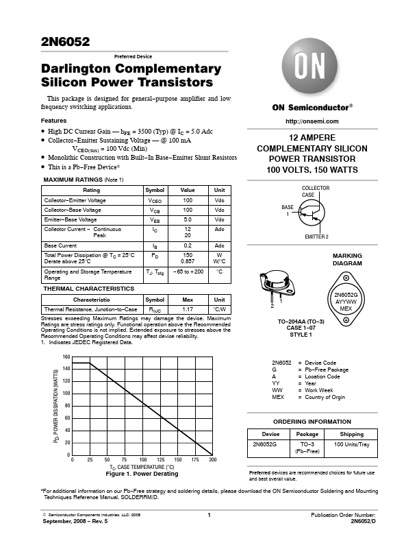
PD, POWER DISSIPATION (WATTS)
160
2N6052 = Device Code
140
G
= Pb−Free Packag...