Dual N-Channel JFET High Frequency Amplifier
CORPORATION
2N5911 / 2N5912
FEATURES ABSOLUTE MAXIMUM RATINGS (TA = 25oC u...
Dual N-Channel JFET High Frequency Amplifier
CORPORATION
2N5911 / 2N5912
FEATURES ABSOLUTE MAXIMUM RATINGS (TA = 25oC unless otherwise specified) Gate-Drain or Gate-Source
Voltage . . . . . . . . . . . . . . . . -25V Gate Current . . . . . . . . . . . . . . . . . . . . . . . . . . . . . . . . . 50mA Storage Temperature Range . . . . . . . . . . . . . -65oC to +200oC Operating Temperature Range . . . . . . . . . . . -55oC to +150oC Lead Temperature (Soldering, 10sec) . . . . . . . . . . . . . +300oC Power Dissipation Derate above 25oC
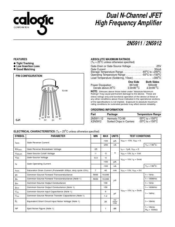
TO-99
Tight Tracking Low Insertion Loss Good Matching
PIN CONFIGURATION
One Side 367mW 3.0mW/ oC
Both Sides 500mW 4.0mW/ oC
NOTE: Stresses above those listed under "Absolute Maximum Ratings" may cause permanent damage to the device. These are stress ratings only and functional operation of the device at these or any other conditions above those indicated in the operational sections of the specifications is not implied. Exposure to absolute maximum rating conditions for extended periods may affect device reliability.
ORDERING INFORMATION Part CJ1
C S2 G1 D2 D1 G2 S1
Package Hermetic TO-99 Sorted Chips in Carriers
Temperature Range -55oC to +150oC -55oC to +150oC
2N5911-12 X2N5912
ELECTRICAL CHARACTERISTICS (TA = 25oC unless otherwise specified)
SYMBOL IGSS BVGSS VGS(off) VGS IG IDSS gfs gfs gos goss Ciss Crss en NF Gate Reverse Current Gate Reverse Breakdown
Voltage Gate-Source Cutoff
Voltage Gate-Source
Voltage Gate Operating Curr...