2N5772
2N5772
NPN Switching Transistor
• Sourced from process 22.
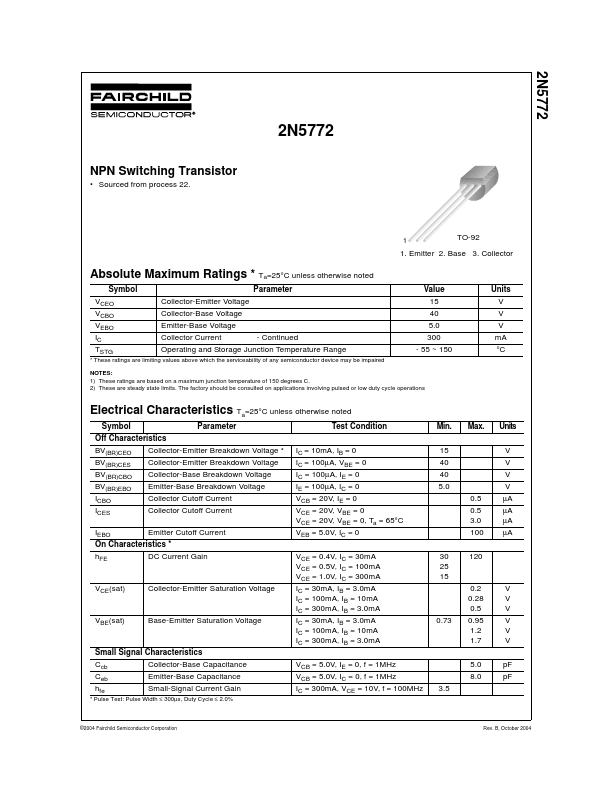
1
TO-92
1. Emitter 2. Base 3. Collector
Absolute ...
2N5772
2N5772
NPN Switching Transistor
Sourced from process 22.
1
TO-92
1. Emitter 2. Base 3. Collector
Absolute Maximum Ratings * Ta=25°C unless otherwise noted
Symbol VCEO VCBO VEBO IC TSTG Parameter Collector-Emitter
Voltage Collector-Base
Voltage Emitter-Base
Voltage Collector Current - Continued Operating and Storage Junction Temperature Range Value 15 40 5.0 300 - 55 ~ 150 Units V V V mA °C
* These ratings are limiting values above which the serviceability of any semiconductor device may be impaired NOTES: 1) These ratings are based on a maximum junction temperature of 150 degrees C. 2) These are steady state limits. The factory should be consulted on applications involving pulsed or low duty cycle operations
Electrical Characteristics Ta=25°C unless otherwise noted
Symbol Off Characteristics BV(BR)CEO BV(BR)CES BV(BR)CBO BV(BR)EBO ICBO ICES IEBO hFE Parameter Test Condition IC = 10mA, IB = 0 IC = 100µA, VBE = 0 IC = 100µA, IE = 0 IE = 100µA, IC = 0 VCB = 20V, IE = 0 VCE = 20V, VBE = 0 VCE = 20V, VBE = 0, Ta = 65°C VEB = 5.0V, IC = 0 VCE = 0.4V, IC = 30mA VCE = 0.5V, IC = 100mA VCE = 1.0V, IC = 300mA IC = 30mA, IB = 3.0mA IC = 100mA, IB = 10mA IC = 300mA, IB = 3.0mA IC = 30mA, IB = 3.0mA IC = 100mA, IB = 10mA IC = 300mA, IB = 3.0mA VCB = 5.0V, IE = 0, f = 1MHz VCB = 5.0V, IC = 0, f = 1MHz IC = 300mA, VCE = 10V, f = 100MHz 3.5 0.73 30 25 15 Min. 15 40 40 5.0 0.5 0.5 3.0 100 120 Max. Units V V V V µA µA µA µA Collector-Emitter Breakdown
Voltage * Collector-Emitte...