2N5322 2N5323
SMALL SIGNAL PNP TRANSISTORS
s
s s
SILICON EPITAXIAL PLANAR PNP TRANSISTORS MEDIUM POWER AMPLIFIER NPN C...
2N5322 2N5323
SMALL SIGNAL PNP TRANSISTORS
s
s s
SILICON EPITAXIAL PLANAR PNP TRANSISTORS MEDIUM POWER AMPLIFIER NPN COMPLEMENTS ARE 2N5320 AND 2N5321
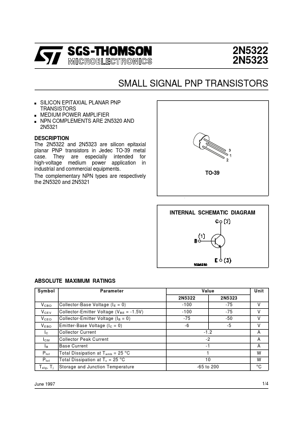
DESCRIPTION The 2N5322 and 2N5323 are silicon epitaxial planar PNP transistors in Jedec TO-39 metal case. They are especially intended for high-
voltage medium power application in industrial and commercial equipments. The complementary NPN types are respectively the 2N5320 and 2N5321
TO-39
INTERNAL SCHEMATIC DIAGRAM
ABSOLUTE MAXIMUM RATINGS
Symbol V CBO V CEV V CEO V EBO IC I CM IB P tot P tot T stg , T j Parameter 2N5322 Collector-Base
Voltage (I E = 0) Collector-Emitter
Voltage (V BE = -1.5V) Collector-Emitter
Voltage (I B = 0) Emitter-Base
Voltage (I C = 0) Collector Current Collector Peak Current Base Current Total Dissipation at T amb = 25 o C Total Dissipation at T c = 25 o C Storage and Junction Temperature -100 -100 -75 -6 -1.2 -2 -1 1 10 -65 to 200 Value 2N5323 -75 -75 -50 -5 V V V V A A A W W
o
Unit
C
June 1997
1/4
2N5322/2N5323
THERMAL DATA
R thj-case R thj-amb Thermal Resistance Junction-Case Thermal Resistance Junction-Ambient Max Max 17.5 175
o o
C/W C/W
ELECTRICAL CHARACTERISTICS (Tcase = 25 oC unless otherwise specified)
Symbol I CBO I EBO V (BR)CEV Parameter Collector Cut-off Current (I E = 0) Collector Cut-off Current (I C = 0) Collector-Emitter Breakdown
Voltage (V BE = 1.5V) Test Conditions V CB = -80 V V CB = -60 V V EB = -5 V V EB = -4 V I C = -100 µ A for 2N5322 for 2N5323 I C = -10 mA for 2N...