2N2222A
Small Signal Switching Transistor
NPN Silicon
Features
• MIL−PRF−19500/255 Qualified • Available as JAN, JANTX, ...
2N2222A
Small Signal Switching Transistor
NPN Silicon
Features
MIL−PRF−19500/255 Qualified Available as JAN, JANTX, and JANTXV
MAXIMUM RATINGS (TA = 25°C unless otherwise noted)
Characteristic
Symbol Value
Unit
Collector −Emitter
Voltage
Collector −Base
Voltage
Emitter −Base
Voltage
Collector Current − Continuous Total Device Dissipation @ TA = 25°C Total Device Dissipation @ TC = 25°C Operating and Storage Junction Temperature Range
VCEO VCBO VEBO
IC PT PT TJ, Tstg
50 75 6.0 800 500 1.0 −65 to +200
Vdc Vdc Vdc mAdc mW W °C
THERMAL CHARACTERISTICS
Characteristic
Symbol Max Unit
Thermal Resistance, Junction to Ambient
RqJA
325 °C/W
Thermal Resistance, Junction to Case
RqJC
150 °C/W
Stresses exceeding those listed in the Maximum Ratings table may damage the device. If any of these limits are exceeded, device functionality should not be assumed, damage may occur and reliability may be affected.
http://onsemi.com
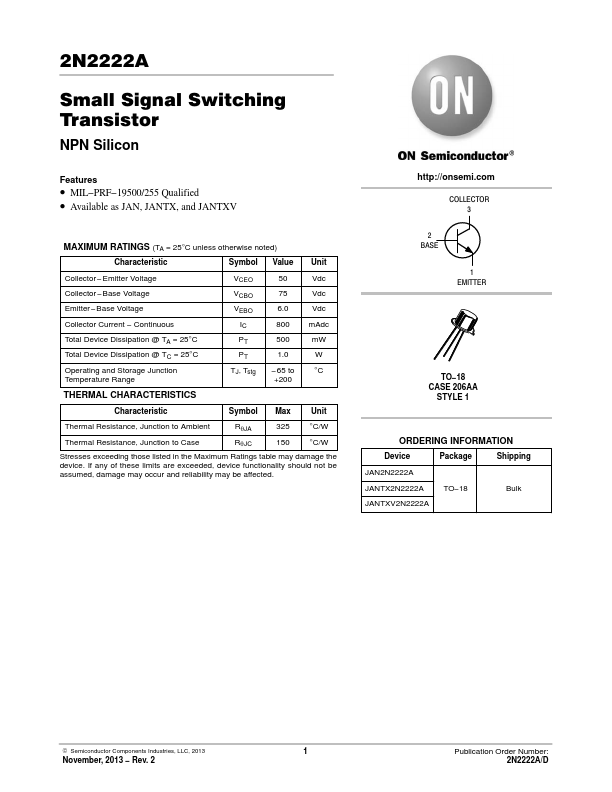
COLLECTOR 3
2 BASE
1 EMITTER
TO−18 CASE 206AA
STYLE 1
ORDERING INFORMATION
Device
Package
Shipping
JAN2N2222A
JANTX2N2222A TO−18
Bulk
JANTXV2N2222A
© Semiconductor Components Industries, LLC, 2013
November, 2013 − Rev. 2
1
Publication Order Number: 2N2222A/D
2N2222A
ELECTRICAL CHARACTERISTICS (TA = 25°C unless otherwise noted) Characteristic
Symbol
Min Max
Unit
OFF CHARACTERISTICS
Collector −Emitter Breakdown
Voltage (IC = 10 mAdc)
V(BR)CEO
50
−
Vdc
Collector−Base Cutoff Current (VCB = 75 Vdc) (VCB = 60 Vdc)
Emitter−Base Cut...